Engineering 100-980
Lab 7: Designing a PCB using Altium Designer
Contents
Introduction
In this lab, you will be designing a PCB using Altium Designer, an industry-standard PCB design software. It’s crucial to focus on creating a high-quality design, as changes cannot be made to a PCB after the design is sent off to be manufactured.
There is no post-lab for this lab, but you will be reviewing each other’s PCBs. Focus on making sure your design is good, and everything about your board works. Upon submission, if you fail any design rule checks, you will receive points off this lab. This is true even if everything else is correct. You must pass all design rule checks to get full credit for this lab.
Participation
Working at a computer often can become a one person deal. It is important to avoid this during the lab. Our goal is for all students in this course learn the basics of Altium. When you are working on your PCBs, have at least one person spotting the person at the computer. This will help you share the work that goes into creating the PCB and eliminate mistakes that can render your finished product useless. It is important that no team member works alone, even during office hours.
Lab Timeline
- October 21st, 2025, 11:59pm: Initial PCB design submission.
- October 28th, 2025, 11:59pm: Peer review submissions due.
Altium
You may want to try to work through the complete Altium tutorial in the Lab 1 post lab. You worked through the schematic in Lab 1. It would be worthwhile to revisit this and then try to make the PCB, since that is what you will be doing in this lab. Note that this walk through is on Canvas in the Files section. (Labs -> Altium Resources -> “Altium - Getting Started.pdf”).
Altium as a software can be very complex, and as such, we have given you some tools to help simplify the process of constructing your PCB. The following pictures are taken from a free online tutorial provided by Altium: From Idea to Manufacture. You can learn more about this example there.
Broadly, the workflow in Altium is divided up into three steps: Schematic, PCB, and Design Rule Check. The Schematic step is where you lay out the electrical schematic of your board. Using all the components, you define how they connect to each other, ground, and power. The PCB step is where you the physical layout of those components on the board. The electrical connections you set up in the schematic are shown for your reference, and you lay them down on your PCB physically as traces. That is, each trace you set corresponds to an electrical connection you outlined in your Schematic. The Design Rule Check step is when the software looks over your work and makes sure you aren’t committing any errors or contradictions. This is inevitably the most frustrating part of using Altium, because you think you’ve done everything right, and the software is here to tell you that you haven’t. It is important to note that design rule checks do not check whether you laid out your board the way you wanted, they will not notice if you accidentally connected your temperature sensor to your pressure sensor instead of the Arduino. You must double check this yourself. The design rule checks only check if your design rules are violating the physical and electrical laws associated with making a PCB.
Schematic
Background
You begin with an idea. A circuit or device that you’d like to realize in a PCB. The first thing you need to do is tell Altium the components you’ll be using, and their relationships to one another. Consider the drawing of a ‘self-running a stable multivibrator’ below.
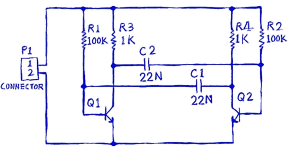
Figure 1: A drawing of a schematic, that pretty closely resembles a schematic you’d make in Altium.
Fig. 2 shows Fig. 1 as an Altium schematic. The schematic is defined in a document with the extension .SchDoc.
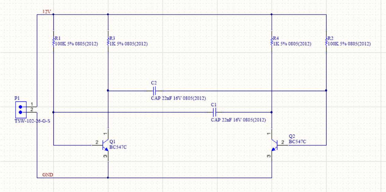
Figure 2: The schematic of an astable multivibrator as displayed through Altium.
For additional reference, here is the schematic you made following Lab 1:
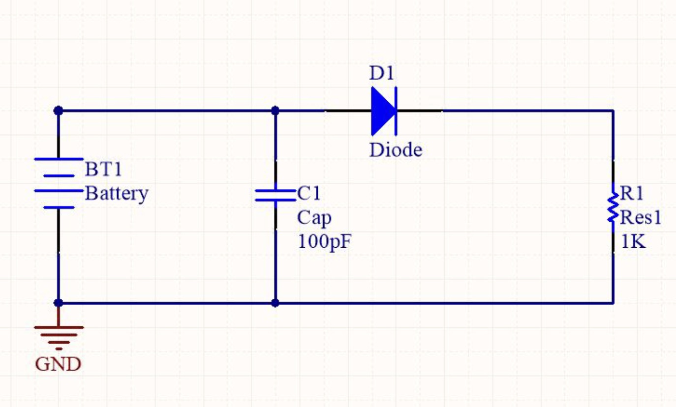
Figure 3: The schematic completed in the Postlab 1 assignment
Note that each component is defined with its own individual symbol. Capacitors, resistors, and transistors (Q1 and Q2), and some connectors (P1) are standardized and thus have pre- loaded symbols in the software, but for most of our components, that is not the case. We have additional libraries custom made by ENGR100 staff with our components pre-loaded, so as we will discuss in the procedure, you can simply drag and drop them into place. Make sure that your team is using the schematic components from the ENGR100 .SchLib files. Using the Simulation Generic Components library will cause issues down the road.
Your Schematic Contents
Obviously, the functionality we’re trying to put on a PCB is the ability to record data from a model rocket, so starting your schematic off by adding your full Lab 5 circuit is a good starting point. Additionally, we decided that turning on and off your board would be nice, so add the SW-SPST switch included in the miscellaneous devices library between the positive terminal of the battery and the VIN pin on the Arduino.
LEDs are also useful when diagnosing software bugs without a computer, telling you if the board is on or off, and also making cool light patterns. Please wire LEDs from the 5v, 3.3v, and 9v battery lines through a resistor and to ground. Please wire any remaining digital pins to their own LED with a 1K resistor on each LED. This way, you have some LEDs to diagnose problems and play with.
It is extremely helpful to draw this out on a piece of paper first. Remember, the schematic is only an electrical connectivity diagram - it doesn’t describe where things are located. So, your schematic doesn’t have to look like the PCB, it just has to have all of the components connected together in the correct way.
In summary, your schematic (and the PCB) must have:
- An Arduino Nano (Classic or Every is fine, they have the same pinout/footprint)
- BME sensor (humidity, pressure, and temperature)
- Accelerometer
- SD Card writer
- LEDs with resistors from 3.3V, 5.0V, and battery voltage lines to ground
- LEDs on any remaining digital pins with resistors
- SW-SPST switch for battery toggle
- Voltage divider to read battery voltage
- Any other components from lab 5 circuits
Procedure: Starting Your Design and Creating A Schematic
- Download the resources provided here. There should be 1 folder called ‘New Altium Libraries’ for you to download.
- Open Altium Designer on a CAEN computer. Navigate to File -> New -> Project…
- Choose the PCB project type.
-
The “Folder” field allows you to choose where this folder is created. You can save it to your “Documents” folder for it to sync across all CAEN instances or, you can navigate to “This PC” -> “U-M Google Drive (I:)” as shown in Fig. 5 and save it in a folder here so that you can share it with teammates. Just be sure that whatever you do, do not save the project in your Downloads folder. On CAEN machines, this location is wiped every 24 hours.
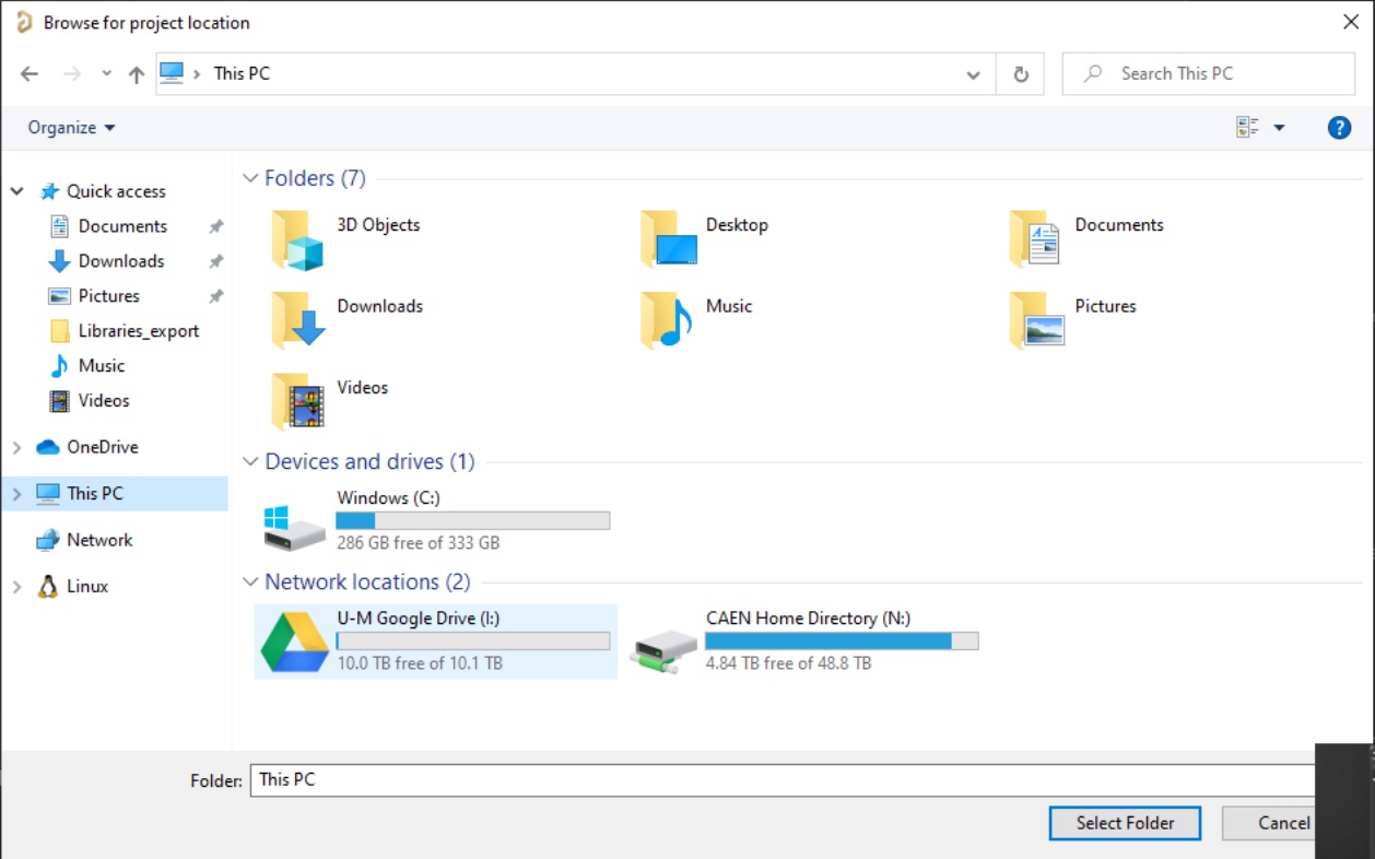
Figure 4: CAEN File Explorer
-
Name your project with your team number and name, and click “OK”. See Fig. 6 for an example Project Creation.
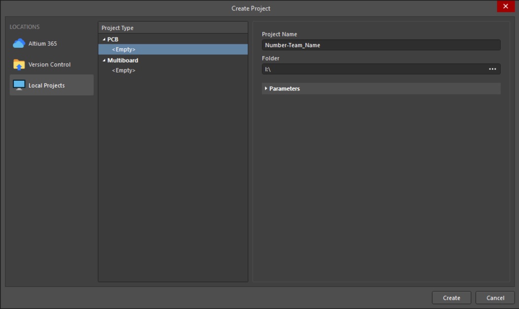
Figure 5: Project Creation Wizard popup
-
Now you should add two libraries we will give you. To do this, go to the Projects tab on the left side of the screen. A picture of this tab is shown in Fig. 7. If you see something else here, see if you can click the word “Projects” at the bottom left of the window.
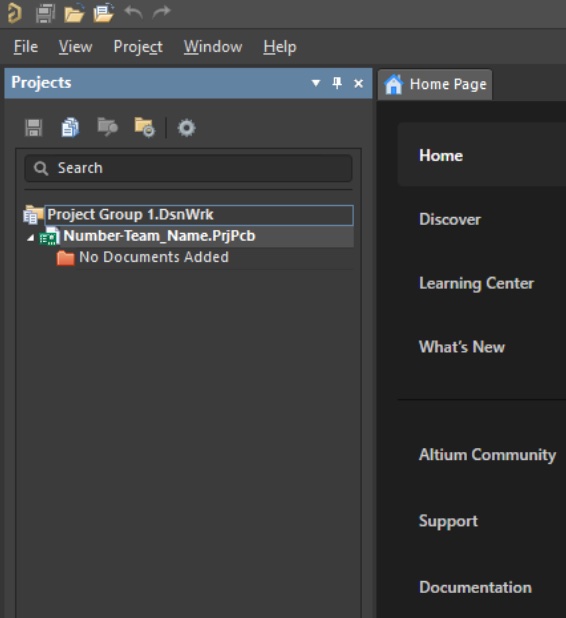
Figure 6: Project Tab
- Right click your project name in bold and click Add Existing to Project. Navigate to your saved PCB libraries and select both of them.
-
Look at the Projects Tab on the left side of the screen. Right click your project name in bold and click Add New to Project -> Schematic. A blank piece of paper should appear on the screen. This is where you are to lay out your schematic drawing. A few instructions for laying out a schematic:
-
Go to Place -> Part to place a component. Navigate to the library you would like to use with the dropdown menu. A keyboard shortcut is to simply press “P” twice in a row.
-
You can either connect everything together with wires or use “nets”. Nets are a convenient way to connect two pins without explicitly drawing a wire between them. You can place a net using Place -> Net Label. This is a great way to make sure things don’t get too messy. One issue with nets is that it may be hard to see what is connected to what. The most common net is ground - it is so common that there is a special button for it. You can click on the ground (GND) button and attach this to all of the ground pins on all of your components. This tells Altium that they are all connected together to a ground pin.
-
You can also use wires to connect everything together. Wires can cross each other without connecting, but if they have a circle where they cross, they are connected. Make sure only the things that are supposed to be connected are connected!
-
To find the properties of a given component, double click its symbol on the schematic. A component-specific properties window will open up. Here you can adjust the part label, the value of the component (such as resistance or capacitance), and the footprint of the component. The footprint is a representation of how the component looks in real life - e.g. what actually will be on your board. You can add a footprint by clicking the corresponding Add button in the Component Properties window.
-
That’s a lot to keep in mind! The path to success involves moving slowing and methodically through each component, writing out your schematic on paper beforehand, staying organized, and asking questions. If you’re confused on what to do, please ask! When you’ve finished your schematic, ask an IA to check it off and make sure it is correct. Once they mark it off, you can move onto creating the PCB. It is in your best interest to have a clean and accurate schematic before moving forward. Even minor changes on the schematic can require substantial changes on your PCB to accommodate.
It is a good idea to design your schematic and then save everything. Make sure that you can quit out of Altium and read back in the schematic. If, for some reason, you need to stop working on this, the end of the schematic creation is a good place to pause.
It is also a good idea to have one of the IAs, teaching instructors, or another group member look over your schematic. Once you start the PCB design, it is harder to go back and modify the schematic - this can be done, but it complicates things.
PCB
Background
The PCB is designed as a separate document with the extension .PcbDoc. We can create a new PCB document and correlate it to our schematic. This will import all the components to the PCB document. Then, just as in the schematic document, we can manually place each footprint. As before, the footprints will be provided via a custom library we have prepared for you.
Note the white lines that connect each of the footprints in Figure 3. These represent what pins on each part that should be connected via traces. This should be done manually, similar to how wires were drawn in the schematic. One notable difference is that physical traces should never be drawn at right angles - instead, they should be at obtuse angles. This is to minimize field leakage and reflection at corners. It is important to note: all 1 kOhm resistors must use a 1206 footprint. If your resistors do not use this footprint by default, switch the footprint to the ‘C1206’ footprint in the miscellaneous devices library using the properties window.
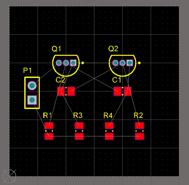
Figure 3: The PCB Layout in Altium
Procedure: Designing the PCB
Pressing 1 on your keyboard takes you to the board design view. Pressing 2 takes you to the component layout screen. Pressing 3 takes you to the cartoon mockup screen. You should do your layout work (e.g. most of the work) in mode 2.
- To create a new PCB file, right click your project name under your Projects tab, click New -> Add New to Project -> PCB.
- Import your schematic components. Go to Design -> Import Changes from Project name. Validate your changes, make sure you see only green check marks next to each change. Then execute them. By zooming in and out on your board (by pressing the mouse scroll button and moving around), you should see a big red box containing all of the components. You can drag and drop them onto the board, which is the black rectangle. If you want to rotate a component, click and hold on it and then press the spacebar. Another option is to click it and press M, which will bring up a menu for moving components. One of these menu options is the ‘rotate selection’ feature. This is better if you want to rotate it a specific amount and not in increments of 90 degrees.
- Now we should adjust the size of our board. To do this, press 1 on your keyboard. Navigate to Design -> Edit Board Shape. The board should be no bigger than 2 inches by 4 inches. You can toggle between Imperial and Metric units by pressing Q. This shows you how to do that.
- We will add some design rules. Press 2 on your keyboard to ensure that you are on the component layout screen. Navigate to Design -> Rules. A PCB rules window should pop up. Set the following design rules:
- Electrical -> Clearance = 6 mil
- Routing -> Width
- Minimum Width = 6 mil
- Preferred Width = 15 mil
- Maximum Width = 30 mil
- Manufacturing -> MinimumAnnularRing = 7 mil
- Manufacturing -> HoleSize = 13 mil (min) and 125 mil (max)
- Layout your components neatly on the board. Be sure to place your Arduino and Data Logger in such a way that you do not obstruct the port for the uploading cable or the SD Card opening.
- To connect traces to your different components, navigate to Route -> Interactive Routing. When you are placing a trace press 3 to toggle between your min, preferred, and max trace width as set in the design rules. Recall from lecture that your board will contain two copper layers. These layers are referred to as the top and bottom layers, and are colored red and blue. Route all traces except the ground traces. We will route those later to our polygon pour ground plane, which we make last.
- You can place labels on your PCB to help you remember things. Because LEDs are directional, you may want to indicate which sides are positive by adding a “+” label near the high voltage side. Labels are good.
- When routing, all traces should default to 15mil if you implemented the Design Rules correctly. However, you should manually the trace from the +9V connection to the VIN pin on the Arduino thicker, to compensate for the increased current flow through it.
- Pour a ground plane. Using the menu at the bottom of the PCB, select the bottom layer and cover it with a grounded polygon pour. You can now connect all your ground connections directly to this by using vias (no traces involved).
Finally, we have a completed board! Altium creates a cartoon (Figure 4) that we can view before moving on to the final stage: Design Rule Check.
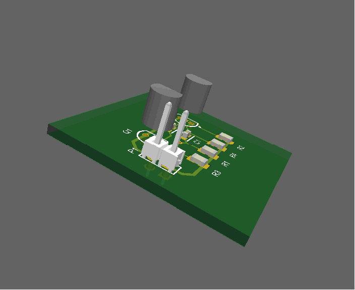
Figure 4: Completed PCB
DRC
The DRC, or Design Rule Check is a way to check the validity of your PCB with respect to the Design Rules we create. More on this in the procedure.
Procedure: Design Rules Check
- Recall that you created a set of Design Rules before creating your PCB. The Design Rule Check (DRC) assesses your design in light of these rules, and highlights any discrepancies between your layout and those rules. Your DRC must return ZERO errors before your PCB can be considered complete. Design Rule Check can be run by navigating to Tools -> Design Rule Check. Click Run Design Rule Check to run DRC. Generally, errors are highlighted in bright green.
- Once you have passed all design rule checks, take a screenshot of your error-free DRC screen.
Final Deliverable
Each team must upload a single zip file containing all project files and a screenshot showing all DRCs passed to the Canvas assignment called “Altium Assignment Uploads” by 11:59pm on October 21st, 2025. Make sure that your PCB passes all design rule checks before submitting it. Each student will peer review three PCBs with rubrics provided on Canvas.
The zip file must:
- Contain all information so that another person can unzip the file, open Altium, and see you schematic and PCB.
- Be named with the following template: team_xx_altium.zip, which xx is your team number expressed as two digits (e.g., 01, 02, 10, 11, etc.)
Peer Review
After the lab, every student will be required to peer review the PCBs of three other teams.
Peer reviews are due by 11:59pm on Tuesday, October 28th, 2025. Each person on your team will personally review the PCBs of three other teams. You will evaluate each one by filling out a Google Form that will be published later in the week. You will be assigned the three teams to review. Note that you will fill out the form once for each PCB you review, so you will submit the form three times.
Peer Review and Final Submission
- Submit your error-free DRC screenshot and all project files to the designated Google Drive folder by October 21st, 2025, 11:59pm.
- Peer review three other teams’ PCBs using provided rubrics by October 28th, 2025, 11:59pm.
Remember, accuracy and collaboration are essential. Reach out to the IAs or the #lab-help channel on Slack for assistance if needed. Good luck with your PCB design!